
Introduction
BGA reballing is a core micro-soldering technique utilized in mobile phone motherboard repair, employed to resolve issues such as poor chip connections, failure to power on, and aging solder joints. The repair process requires precise control over temperature, stencil alignment, and solder ball formation to restore the chip’s electrical connectivity. By utilizing specialized tools—including anti-static workstations, high-quality solder paste, and Mechanic reballing stencils—technicians can execute chip reballing and motherboard repairs with greater consistency, thereby enhancing both the success rate and long-term stability of device repairs.
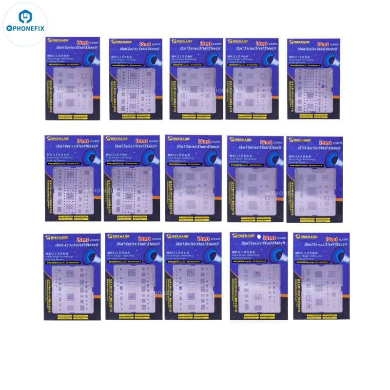
Understanding BGA Reballing and Required Tools
BGA reballing refers to replacing old solder balls with new ones under the chip to address proper connectivity between the chip and the motherboard. The method requires an anti-solid-static workbench to prevent electrostatic discharge, which can damage sensitive IC connectors. Important equipment includes hot air conditioner, solder paste, flux, tweezers, solder wick, and mechanics solder stencil designed specifically for chip size The stencil ensures uniform ball placement, which is critical for strong overall performance after reinstallation.
The choice of solder paste is extremely important because it determines how smoothly the bubbles form at all heating conditions. Most technicians decide on no-easy lead or lead solder paste based on the needs of the board. Flux plays a key role in aiding solder flow easily and stopping oxidation during heating. A proper BGA Soldering Guide Chip Soldering Stencil Selection Cell Phone Motherboard Repair technique always begins offevolved by deciding on the right gear and preparing an easy, organized workspace that helps accuracy and protection for permanent restoration type.
Preparing the Motherboard and Safe Disassembly
Before starting the rewrapping, carefully remove the motherboard from the machine using the correct disconnect gear. Plastic pry tools and precision screwdrivers are preferred to avoid damage to connectors or protective components. Once the board is uncovered, place it on an Anti-static workbench to ensure safe handling. The defective BGA chip area should be diagnosed, and the temperature sensitivity of the surrounding additives should be monitored before applying any heat treatments .
To remove the BGA chip, a controlled hot air temperature between 330°C and 380°C is usually used depending on the board type and solder composition The airflow should be moderate to keep those flying small additives. Fine ESD-safe tweezers are used to gently lift the chip as soon as the solder melts completely. Overpressure should be avoided as it can damage the motherboard pads. Proper heating methods ensure that the chip comes out clean with the copper plates lifting out or causing damage near the channels.
Cleaning and Surface Preparation for Proper Bonding
After removing the chip, dry each motherboard pad and the underside of the chip very thoroughly. A soldering iron is used with low force to remove old solder residue. The iron temperature for cleaning is usually between 280°C and 320°C which is far from dangerous PCB levels. This step ensures that no chipped surface or residual solder interferes with the brand new turning method, it is essential for a strong electrical connection
Isopropyl alcohol is then used to smooth away debris and dirt from each surface. A lint-free cloth or gentle brush will ensure that no particles are left on the countertop. Clean surfaces increase the adhesion of the solder and reduce the risk of blood clots during the reapplication process. Technicians are constantly looking for a clean spot that is dry under magnification to confirm that the pad is flat, vibrant, and ready to stencil This level of schooling immediately affects the final performance value of the restoration method.
Select Stencil with Mechanical Solder Stencil and apply Solder Paste
Choosing the right stencil is the most important step on the path to repackaging. Mechanical solder stencils need to be adapted to the exact BGA chip layout to ensure accurate circular placement. Stainless steel metal stencils are generally preferred because they offer robustness and a distinctive hollow alignment. The stencil is carefully adjusted on the tile, and moderate changes are made to ensure that each pad is centered correctly.
Once straightened, a thin layer of solder paste is quietly applied across the stencil using a plastic scraper or card. The solder paste shall be released in such a way that all openings can be filled with out holes. In addition to preventing the formation of chopped bubbles, excess paste is easily discarded. After the software program, the stencil is easily lifted, leaving a uniform solder paste on each pad. This step is essential because complex software can cause fast circuit or misconnection sometimes within the reheat process.
Recirculation Process: Hot Air Engineering and Temperature Control
Again, it should go with the flow layer, where the solder paste will be made to the right solder balls. The chip is on a heat-resistant floor of an anti-static workbench, and preheating to stabilize the production temperature starts offevolved from about one hundred fifty °C to one hundred 80 °C This prevents thermal surprises and ensures isothermal distribution at all levels of the chip strong and robust joint.
After preheating, the temperature of the new vent rises from 220°C to 260°C depending on whether unleaded solder is used. Ventilation should be carefully controlled to avoid stressful feather formation. As the temperature increases, the offevolved solder paste starts to melt and forms uniform bubbles under the stencil openings. When the chip is finished, it is miles true to cool allowed out amazing ventilation, ensuring a company constant bond between the solder balls and the chip
Check, download and reconnect for a reliable restore
After reflow cooling, the stencil is carefully removed and examined under chip magnification. All soldering irons look uniform, bright and aligned perfectly. Missing or chipped bubbles indicate preference for reconstruction. A one hit rewrap action ensures strong electrical continuity and prepares the chip for reliable reinstallation on the motherboard. It is important that a thorough inspection is carried out before the final assembly takes place.
The re-rounded chip is then placed back onto the motherboard using special alignment tools. A controlled recirculation method is again performed for solder within the vicinity of the chip. After the cool down, the board is checked for capacity, which includes power-return, display output, and gadget stability. Proper testing confirms that the repackaging technology has restored all the average overall performance and reliability of the device.
Conclusions:
BGA reballing is a critical micro-soldering technique employed in the repair of mobile phone motherboards and at the chip level; it effectively resolves cold joints and chip connectivity failures. The repair process requires precise control over temperature, stencil alignment, and heating duration, utilizing high-quality solder paste and specialized reballing stencils to reconstruct the solder balls. Adherence to standardized procedures not only restores BGA electrical connections but also extends the operational lifespan of the device. A skilled command of the reballing process—coupled with the proficient use of specialized tools—constitutes the fundamental basis for enhancing both the success rate and the stability of chip-level repairs.